
An innovation that stabilizes the nanotip used in tip-enhanced Raman spectroscopy (TERS) prolongs the imaging time window well beyond the current 30 minute limit. Scientists have demonstrated that the enhanced system is capable of imaging nanoscale defects over six hours in a micrometer-sized, two-dimensional tungsten disulfide film – a material commonly used in optoelectronic devices. The enhanced imaging technology could open doors for precise, high-resolution imaging of optoelectronic devices and biological samples.
The study1 was led by Ryo Kato, PhD, an assistant professor at the Institute of Post-LED Photonics at Tokushima University, and Takayuki Umakoshi, PhD, an associate professor and Prabhat Verma, PhD, a professor of physics, at Osaka University in Japan.

Kato said, “We have developed a cutting-edge optical microscopy that achieves long-duration nanoimaging with a large field of view and high resolution, which can be applied for versatile samples, including optoelectronic device materials and biomolecules.”
“Our new drift compensated TERS microscopy could not only evaluate surface properties of device materials better but also allow us to study biological processes such as the mechanism underlying the development of diseases. This, in turn, could help develop novel clinical methods and therapies,” said Umakoshi.
Raman Spectroscopy
Raman spectroscopy is a non-destructive optical microscopy technique that exploits the interaction of light with chemical bonds in a sample. The technology provides in-depth information about an object’s chemical structure, phase, crystallinity, and molecular interactions.
However, Raman spectroscopy, like other optical microscopy techniques, is restricted by the “diffraction limit”. This indicates the inability to resolve or separately detect points that are less than half the wavelength of light apart. The diffraction limit prevents such techniques from attaining nanoscale resolutions.
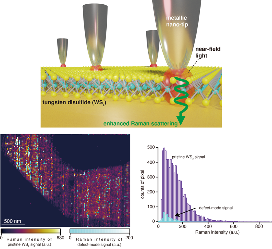
The invention of TERS improved upon conventional Raman spectroscopy. It can reach spatial resolutions below the diffraction limit by confining light in a nanoscale metal tip above the sample being imaged. This enables light to interact with chemical bonds on the surface of the sample. The scattered light is captured and analyzed in the imaging process. TERS can analyze chemical compositions and surface defects in samples at nanoscale resolutions.
Drift limits TERS
However, the nanotip used in the TERS instrument tends to drift from its fixed location both vertically and laterally due to unavoidable thermal and vibrational fluctuations under ambient conditions, causing the sample to either move out-of-focus or misalign between the nanotip and focal spot, or both. This distorts the scattered light signals. To prevent such drift-induced distortion, TERS imaging must be limited within a time window of half an hour. But this prevents imaging of micrometer scale samples at nanoscale resolutions.
“Long time TERS imaging has been one of the grand challenges in the TERS field since its invention in 1999 and its first publication in 2000. TERS suffers from vertical (defocusing) and lateral (blurring) drifts due to its signal-hungry and combined-measurement nature,” said Yung Doug Suh, PhD, a professor of chemistry at the Ulsan National Institute of Science and Technology, in South Korea, who was not involved in the current study. “This work has achieved as long as 6 hours of TERS imaging by the author’s sophisticated instrumentation.”
“Existing optical imaging techniques either allow small-area scanning with nanoscale resolution or large-area scanning with poor resolution. This is because scanning large areas at nanoscale resolution requires significantly longer measurement times and the experimental system cannot maintain stability at nanoscale level for such a long times under ambient conditions,” said Verma. “Inspired by the need for time, we have developed this new and interesting technique by utilizing our homebuilt feedback system that is capable of keeping the experimental system stark stable with nanoscale precision for several hours.”
Tracking the nanotip
In the current study, the scientists have compensated for drifts of the nanotip over periods longer than 30 minutes, by developing a feedback system that tracks the displacement of the focused light source and readjusts the position of the focus plane as needed. In this feedback system, a laser guide beam is directed into the microscope. The displacement of this laser beam’s reflection tracks the focal point of the light source. When the system senses a drift or a change in the focal position of the light source, a piezo-controlled objective scanner stabilizes the focus.
The team designed a laser-scanning-assisted tip drift compensation system to stabilize the nanotip. Galvano-scanners take images of the laser spot around the metallic nanotip just as it approaches the sample surface. This image appears as a bright spot and indicates the position of the nanotip. Once a pixel is measured, the image of the laser spot around the nanotip is recaptured. The laser spot is then moved to match the new position of the nanotip in this image. This process continues throughout imaging and ensures that the nanotip remains fixed.
“This provides extreme stability to the experimental system with nanoscale precision,” said Verma. “This innovative nanoimaging technique dramatically improves the way large sized samples could be imaged with nanoscale resolution for their applications in optoelectronic and other devices.”
Umakoshi said, “This research made a breakthrough on TERS imaging time, which allows one to do imaging forever until it meets another limitation (such as tip oxidation). This potentially enables imaging with an extremely large field of view and imaging some specific samples that has not been possible due to weak Raman signals.”
The enhanced system increased the imaging time window 14-fold over conventional approaches and detected unique defects and a higher density of defects that were missed through conventional TERS imaging.
Next steps
The imaging time window can potentially be extended further. This will enable researchers to explore new applications of the technique and extend it to biological samples that generally yield extremely weak optical signals.
“One could drastically improve the spatial resolution instead of the imaging area, where longer measurement time can be utilized to improve the spatial resolution, perhaps to angstrom scale,” said Verma. Prolonged optical imaging capabilities will enable the detection of rare and novel properties of physical and biological materials.
References
- Kato R., Moriyama T., Umakoshi T. et al. Ultrastable tip-enhanced hyperspectral optical nanoimaging for defect analysis of large-sized WS2 layers.
- Sci Adv (2002). https://www.science.org/doi/10.1126/sciadv.abo4021
